While rummaging through a box of electronic scraps and parts, I found components that were purchased nearly 10 years ago for building a Sinclair ZX80 clone. I was only 15 years old at the time, and though ambition was high, electronics experience was not, and I could never get the first piece of the circuit (the clock oscillator) running.
Those who know about the ZX80 will wonder why a kid in 2008 was interested in a 1980’s computer. It is true, that most interest in vintage computing is held by enthusiasts who are nostalgic for the days when these machines were new. I however hold a general interest in technological history, be it radio, film photography, or vintage computers. These machines were also significantly more approachable than machines are today. When you buy a computer today, you experience its function but very little about its internal workings. In contrast, when a microcomputer was purchased in 1980, it included a complete schematic diagram, ROM listing, memory map, and instructions for programming it in BASIC (or assembly for the adventurous).
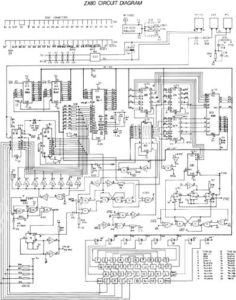
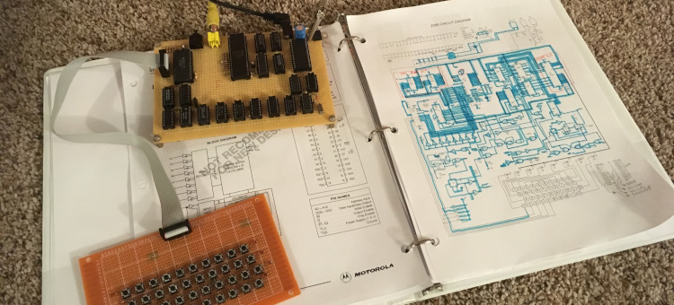
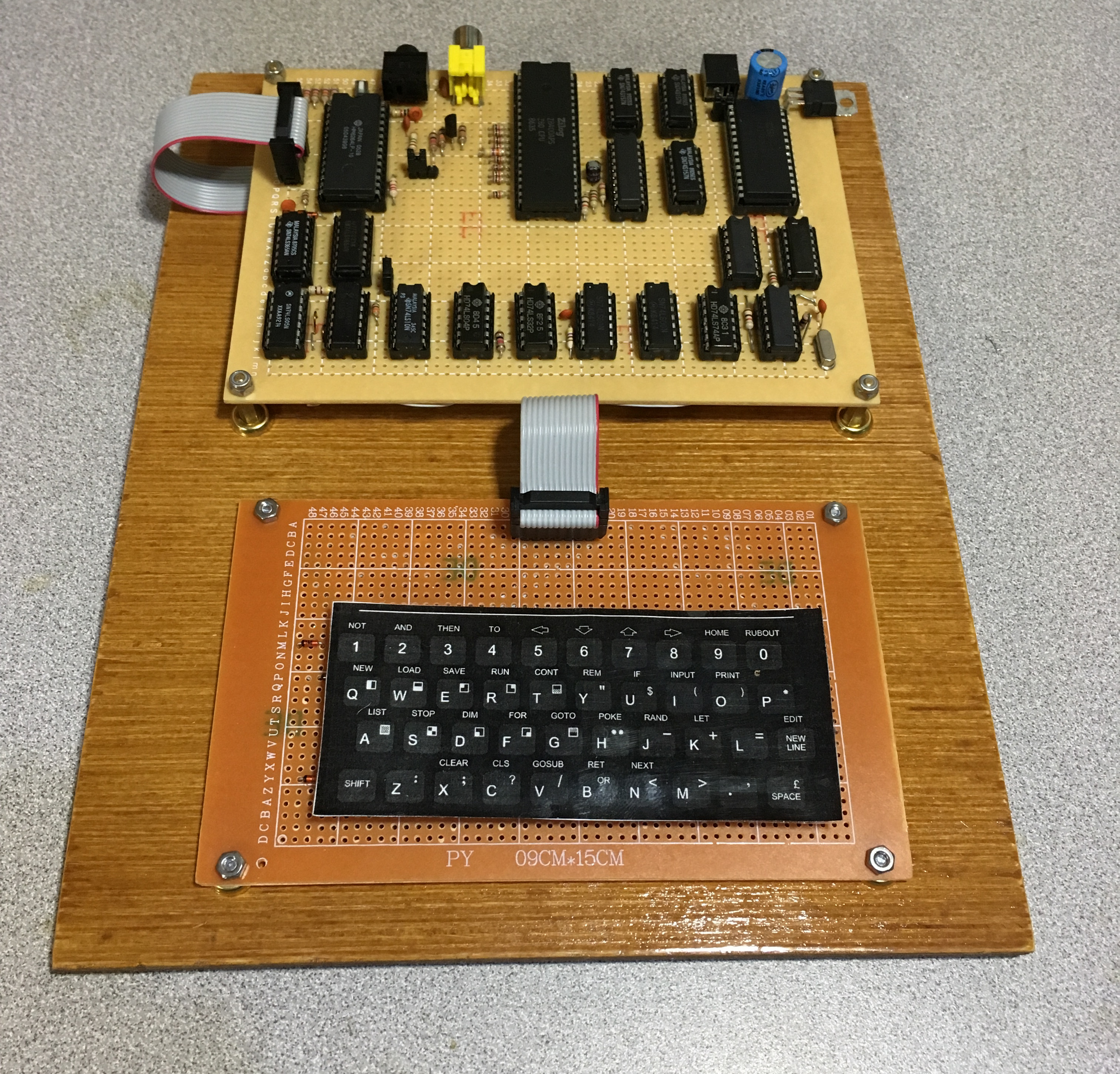
The ZX80 schematic will fit on a single page of paper, and when I stumbled across it in 2007 I was captivated. With nothing more than a Z80 Microprocessor, a static RAM chip, a single parallel EEPROM, and a handful of discrete 74 series logic chips, a complete computer could be constructed!
The history of this particular machine is quite interesting. Designed by Sir Clive Sinclair in 1979, this machine had one goal – to be as inexpensive as possible. While contemporary home computers were several hundred dollars, this machine sold for 79£ as a kit, or 99£ fully assembled. To do this however, some clever tricks were employed, and several sacrifices were made.
The ZX80 had no sound. None that is, other than the 300 baud screeches made when saving programs to an audio cassette tape. Software is cheap, hardware is expensive therefore much of the interface functionality was offloaded to the CPU rather implemented on physical hardware. This means that user code can be executed only when the display is not active, programs are not being loaded or saved, and the keyboard is not being scanned.
These design choices manifest themselves in amusing ways. When entering a BASIC program, the TV display will go blank for a split second upon any keystroke while the input is being processed. When loading programs from a tape, the serialized data is read by some of the same hardware that generates a TV signal, thus noise and interesting line patterns appear on the display while loading. And when a BASIC program is being executed, the screen is dark until an INPUT command is encountered, or the program halts for any reason. While this architecture does allow for simple input, compute, then output type of software, it is hardly a gaming machine.
But it was cheap! And to an electronics hobbyist in the 21st century, it perfect because it contains no custom or proprietary chips.
Just before finals week in the fall of 2018, it hit me, “I’ve had three years of electronics studies,” I thought, “Surely I should be able to finish what I started ten years ago.” So I scrounged the parts out of my junk box, compared them to the BOM, and created a DigiKey order. First however, I needed to see if I could get over the hurtle that had originally halted the project. I built the oscillator and to my complete surprise, it worked the first time. So I placed the DigiKey order.
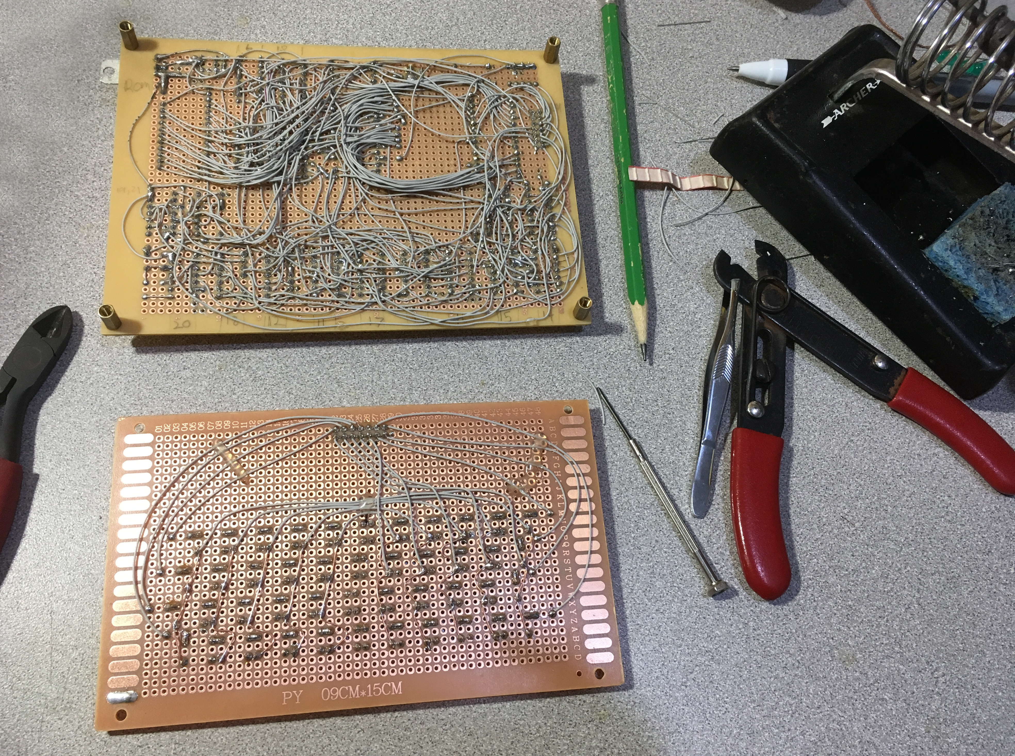
After Christmas I began to layout the IC sockets on the perfboard. It seemed best to follow the layout of the original PCB assuming that with only two layers, the original layout would be as efficient as possible. Finding appropriately sized hookup wire proved difficult. I cringed at the thought of spending $10-20 for only 100′ of solid-core 30 gauge hookup wire. I racked my brain for a few days until I remembered that Ben Heckendorn had used cannibalized 80 pin IDE cables in his hacks when he needed small wire. Junk box to the rescue.
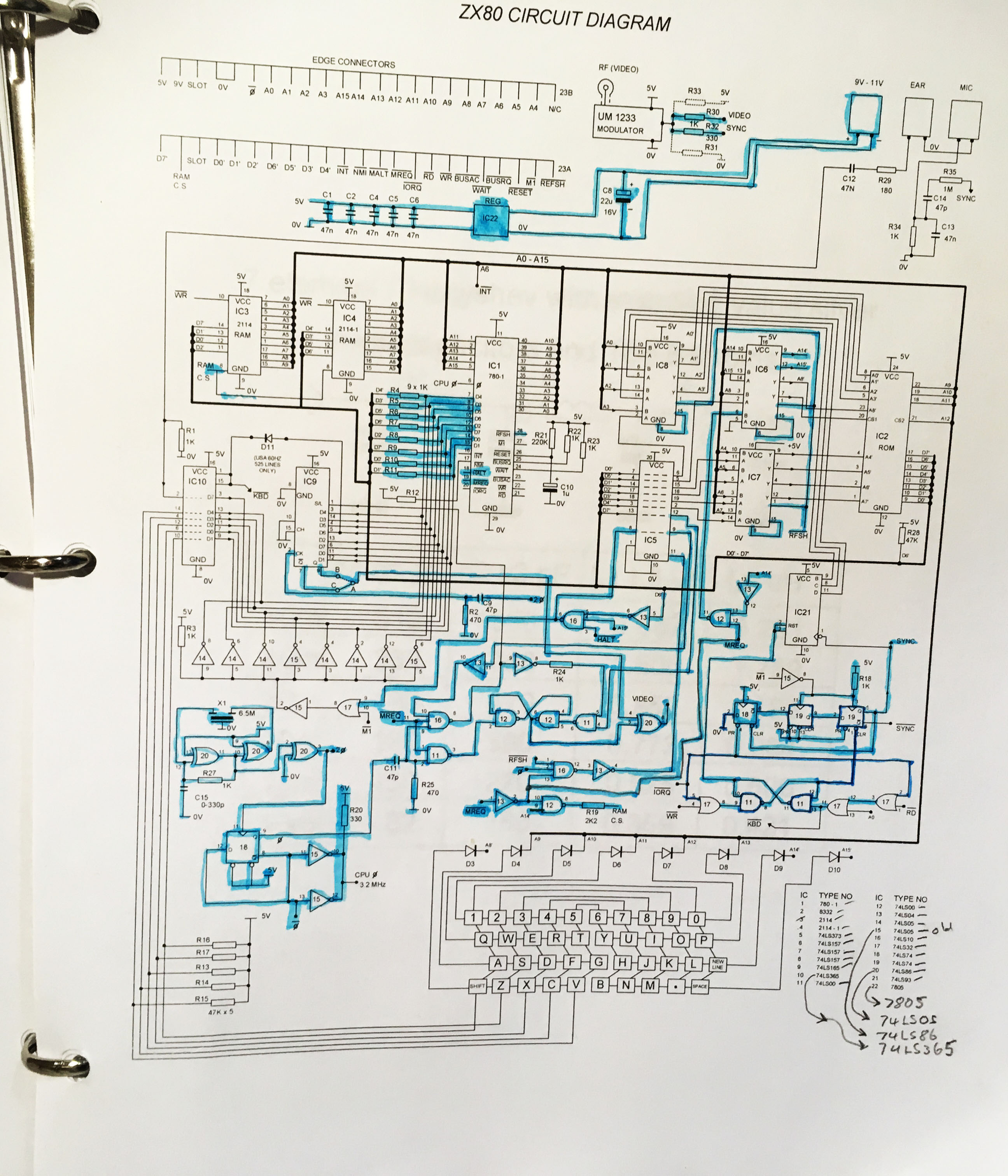
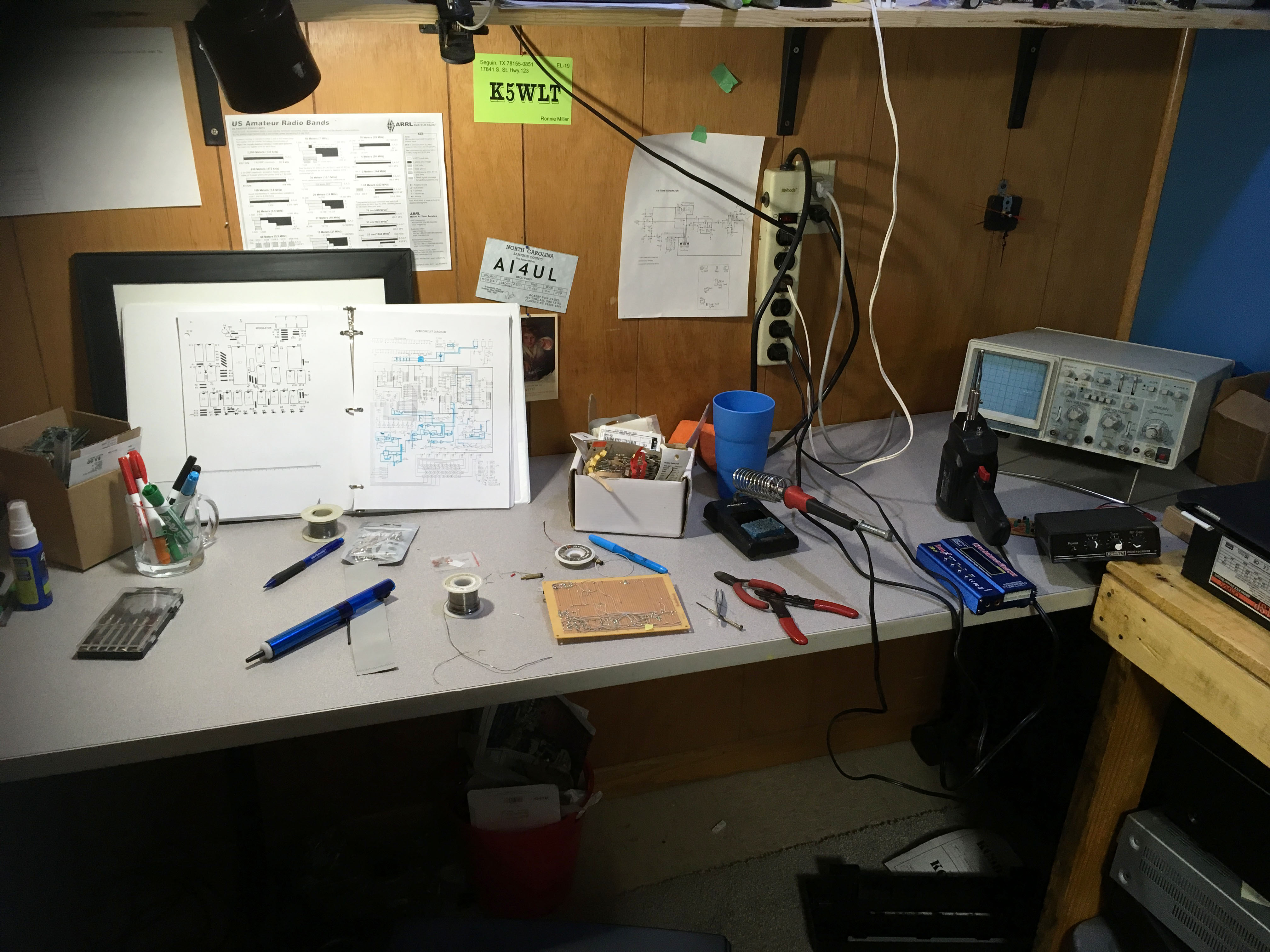
I began wiring the circuit one node at a time, trying to make every connection of that node at once. I would then highlight the node in the schematic, and proceed to the next one. When all of the nodes connecting to a particular IC were completed, I would highlight that IC. After verifying the frequency and amplitude of the clock oscillator, I began to work on the discrete logic in the lower part of the schematic.
Several tricks were developed along the way. First, it was much easier to correctly wire the nodes when I wrote the IC numbers on the bottom side of the perfboard, and labeled pin one. This allowed work to progress without flipping the board over to check that I was soldering to the correct pin.
A modern computer would never function with point-to-point wiring. This is because at high frequencies, wires look more like RF transmission lines than single nodes of constant potential. To stabilize this, modern computer PCBs are designed to have ground planes on every other layer, or even use differential signaling with two identical traces. But at 3.25MHz this is not a problem. Ample time exists for logic inputs to respond to slow rising edges. And even with a 20MHz scope, it was easy to see that most of the lines had little or no ringing.
After about two weeks of regular hours at the bench, I finally declared the wiring complete. This was said however, with the full knowledge that there was most certainly an error someplace. But I did a quick short circuit test for the power supply, and checked positive and negative supply to all chips. After each IC was inserted, I connected the board to a TV, and… there was no display. So the troubleshooting began.
Some of the signals could be easily traced with an oscilloscope, but others require more complex triggering than my simple scope would allow. After some time of probing however, I realized that the whole circuit was operating in a short loop of some sort. Sure enough, the CPU /RESET line was attached not to VCC, but to the /REFRESH line. Thus after reading one instruction, the CPU would reset itself, and repeat. That was easily mended. Still no inverse K on the display however.
As an aside, while many computers of the time would display the letters OK in the screen as a prompt, the ZX80 simply printed K to save a few bytes in the ROM. Go figure.
At this point, things were happening on the board. All of the address and data lines were wiggling, but some systems such as the TV sync generator which is triggered by a CPU I/O request was not running. This led me to believe that the CPU was executing code, it was not executing the right code. Interestingly, on a Z80 CPU, every byte from 0 to 255 is a valid instruction, therefore the CPU will never stall, but simply run random code forever. I removed the ROM, and verified it again in my Arduino EEPROM programmer circuit. Every byte checked out. I placed the RAM chip in the same circuit, and did a series of read/write tests to it. I also removed the Z80 and built a few test circuits. One to execute NOOPs (instruction 0x00) forever, and another to HALT immediately on boot. Both of those tests proved successful. The processor was not damaged in any obvious way.
It was becoming evident that of the 16 address lines, or 8 data lines, some part of the signal was getting lost between the ROM and the CPU. At the time however, I could think of no way to prove this theory, or diagnose the circuit in any way.
I resorted to spending an afternoon doing a “beep test” with a multimeter, going through a fresh printing of the schematic, and highlighting every node that beeped successfully. While I did find a few minor wiring errors, I found nothing that would cause the behavior I was experiencing. I was surprised however to find IC21 on the schematic which is a 74LS93 counter, is not actually powered from the corner pins like most of logic chips. Rather, it is powered from pins 5 and 10 in the middle of the sides. That wiring was fixed, but still no inverse K.
A logic analyzer is the solution that any modern engineer would have suggested. But, such a magnificent piece of test equipment does not exist on my bench, and the electrical engineering labs at the university were closed for the winterim.
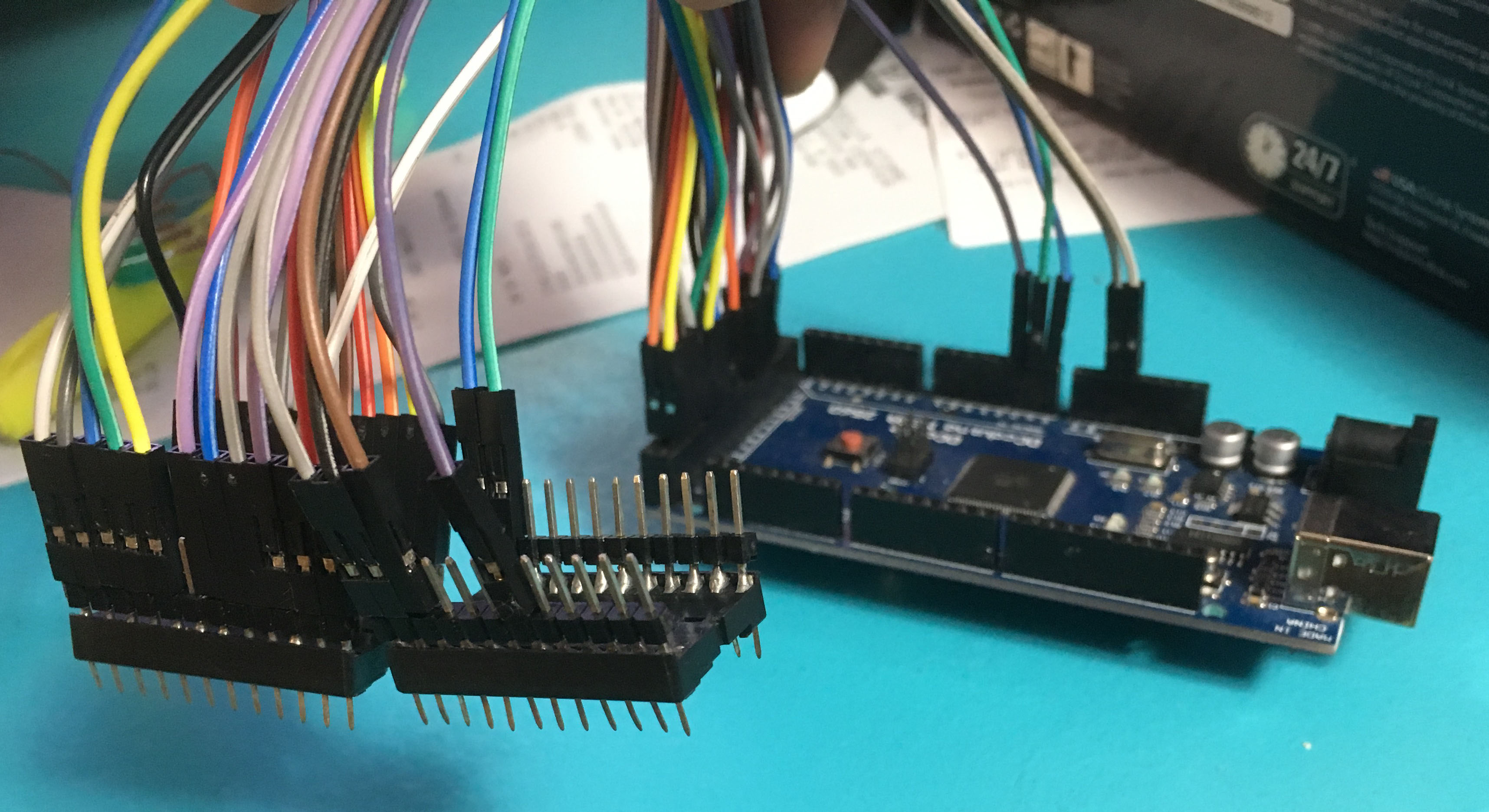
At about 4:30 the next morning an idea hit me. Since the CPU does everything in this circuit, there should be no major reason why I couldn’t replace the CPU with an Arduino with sufficient pins, ignore the incoming clock, and start verifying various systems! I soldered 40 header pins to a couple of wide IC sockets to build an interposer of sorts which I could easily plug into my existing board. I used lots of flux which made the soldering easy, and in a few minutes I was ready to verify the solder joints with a beep test. But something wasn’t right. There was nearly 100 ohms of resistance between adjacent pins on the interposer. This should not be. They should be completely open. I was absolutely horrified to discover that the plumber’s flux I had been using on my entire build would become conductive when heated! This discovery brought on immediate nausea. Weeks of work done had been done fundamentally wrong. Then I remembered cleaning flux from PCBs at my engineering internship. A quart of rubbing alcohol, an old plastic kitchen container, and an old toothbrush were commandeered from around the house, and after removing all of the integrated circuits, I scrubbed both sides of the board as vigorously (and carefully to not disturb the wiring) as I could . The board was then thoroughly dried with a hair dryer.
All of the removed components were replaced, and with shaking, anxious hands, I connected the board to a display. The inverse K appeared.
My wife commented that I was so excited that she was surprised I didn’t scream, waking the sleeping children. (It was nearly 1AM at this point.) But after running for a minute or so, the machine froze, and the display disappeared. Resetting it would sometimes bring it back, but I began to get the impression that something was failing after the machine would heat up. Since the original troubleshooting plan was to replace the CPU with an Arduino, I continued with that quest. The software written for flashing the EEPROM was easily modified to read bytes from the ROM, and compare against the known image.
Things weren’t matching up, a few bytes were correct, but most were not. This told me that the address lines were functioning correctly, but there was an issue with one or more of the data lines. Since the issue was potentially heat related, I put the whole thing in the freezer for a few hours, and then tested it again. No obvious difference. Then I started performing bit-wise comparisons with the bytes the Arduino was reading, with what was in the ROM image. It looked like just a few bits were problematic. I modified the program to perform an XOR between the bytes that were read, and the ROM image, and out came a list of all the problematic data lines.
The wiring of those lines was scrutinized, and sure enough, there were nearly microscopic metal filings or clippings between various solder joints that was shorting them out. I cleaned these areas with an exact-o knife and compressed air, and powered the computer back up. This time it stayed running indefinitely.
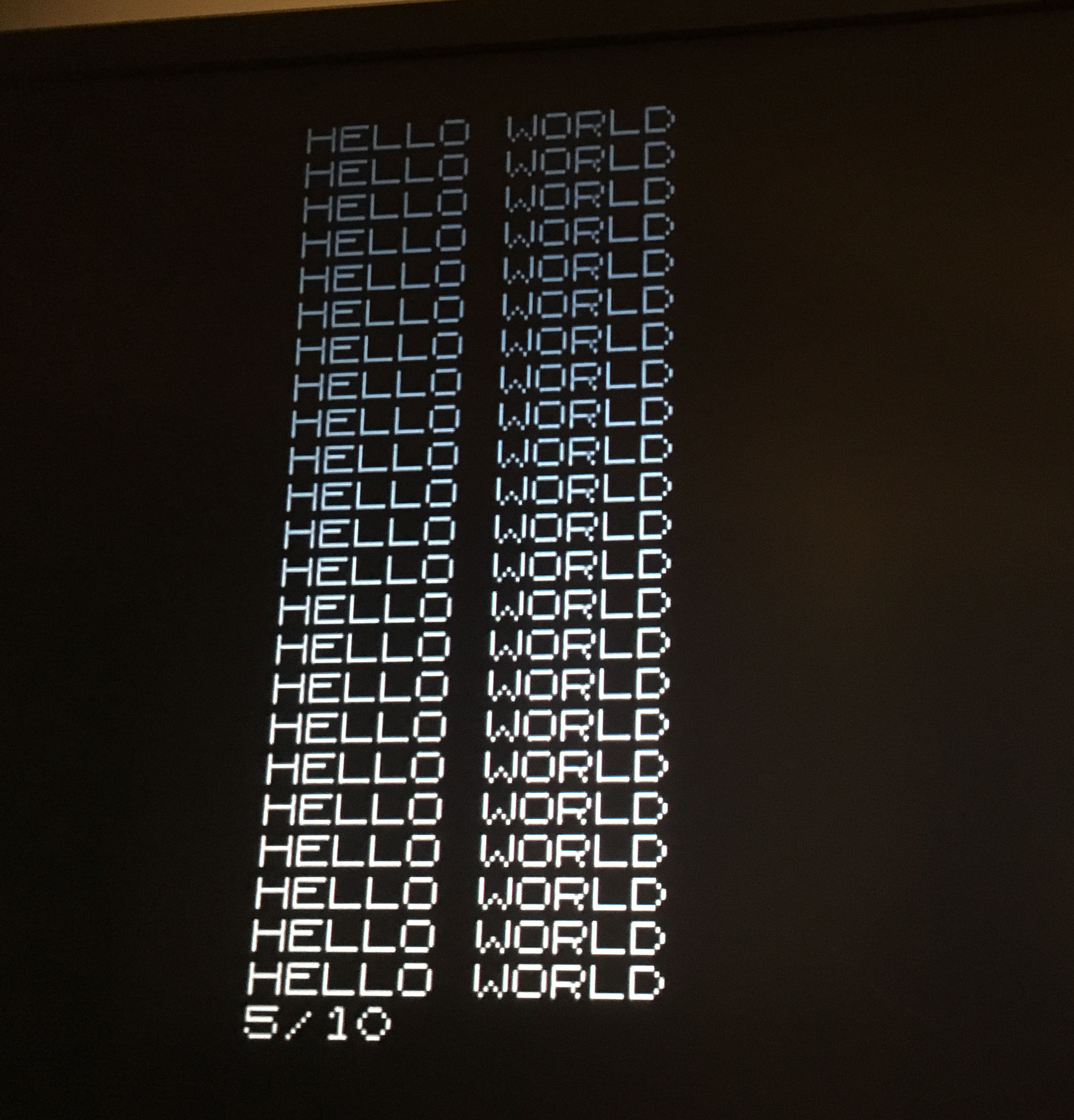
The keyboard matrix was wired up, and I entered a simple program.
10 PRINT "HELLO WORLD"
20 GOTO 10
Aah…. microcomputers!
Among the finishing touches was an amplifier for the audio cassette tape input. Unfortunately, the stock circuit is not sensitive enough to load programs from a PC’s headphone jack. I was about to jump in designing a common collector linear BJT amplifier, when I realized that though this is an audio signal, it is actually digital, and not analog. Thus the amplifier needn’t be linear. So a quick no-calculations biased, BJT switch was wired up on a breadboard, and tested. Sure enough! The ZX80 just loves a distorted, clipped input signal. The circuit was implemented on the main board with a three pin jumper selecting to use the amplifier, or to bypass it.
I borrowed my friend’s impressive looking books about writing “Spacegames for Your Home Computer”, and a green-phosphor monochrome monitor from an Apple III. 8 bits never looked so good!
Finishing a project that I had once given up on brought an immense sense of satisfaction and fulfillment. It has also inspired me. What other projects are lingering that could be completed? Who knows. Maybe the pinball machine.
*I must thoroughly applaud Grant Searle who has done a wonderful job of documenting the ZX80 circuitry, designing upgrades, and re-drawing the original schematics and PCB layouts. His commitment to this information is evident in the fact that his website has – as it advertises – been online since 1996! (Just think, that website is only two years younger than me.) He has also reverse-engineered the ULA chip of the ZX81 and now documents how to upgrade the ZX80 for flicker-free “slow mode.”
Wow! That’s amazing!
Congrats on getting back to (and finishing!) a project you started so long ago. I have a few like that.